Exercise 14.1
In an n-type silicon, which of the following statement is true:
(a)
Electrons are majority carriers and trivalent atoms are the dopants.
(b)
Electrons are minority carriers and pentavalent atoms are the dopants.
(c)
Holes are minority carriers and pentavalent atoms are the dopants.
(d)
Holes are majority carriers and trivalent atoms are the dopants.
Not cross-checked
NCERT prints no numerical answer for this exercise, so this working has not been cross-checked against the book.
NCERT’s answer
(c)
In n-type silicon, tetravalent Si is doped with a pentavalent impurity (e.g., As, P, Sb). Each pentavalent dopant atom contributes one extra electron (beyond the four used in covalent bonding) that is loosely bound and easily goes into the conduction band, so electrons become the majority carriers and holes (from thermally broken bonds) are the minority carriers; the dopant atoms themselves are pentavalent.Correct statement: (c) Holes are minority carriers and pentavalent atoms are the dopants.
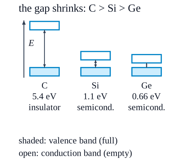 The energy band gap \(\displaystyle E_g\) is the energy separation between the top of the valence band and the bottom of the conduction band. Among the Group-$\displaystyle 14$ elements, the band gap decreases as the atomic size increases (larger atoms hold their valence electrons less tightly, and the overlap/splitting of energy levels into bands is different), going down the column from carbon to silicon to germanium:\[(E_g)_C \approx 5.4\text{-}5.5\ \mathrm{eV}, \quad (E_g)_{Si} \approx 1.1\ \mathrm{eV}, \quad (E_g)_{Ge} \approx 0.66\ \mathrm{eV}
\]So \(\displaystyle (E_g)_C > (E_g)_{Si} > (E_g)_{Ge}\). This is why diamond (carbon) is an insulator, silicon and germanium are semiconductors, with germanium being the more conductive of the two at room temperature.Correct statement: (c) \(\displaystyle (E_g)_C > (E_g)_{Si} > (E_g)_{Ge}\).
The energy band gap \(\displaystyle E_g\) is the energy separation between the top of the valence band and the bottom of the conduction band. Among the Group-$\displaystyle 14$ elements, the band gap decreases as the atomic size increases (larger atoms hold their valence electrons less tightly, and the overlap/splitting of energy levels into bands is different), going down the column from carbon to silicon to germanium:\[(E_g)_C \approx 5.4\text{-}5.5\ \mathrm{eV}, \quad (E_g)_{Si} \approx 1.1\ \mathrm{eV}, \quad (E_g)_{Ge} \approx 0.66\ \mathrm{eV}
\]So \(\displaystyle (E_g)_C > (E_g)_{Si} > (E_g)_{Ge}\). This is why diamond (carbon) is an insulator, silicon and germanium are semiconductors, with germanium being the more conductive of the two at room temperature.Correct statement: (c) \(\displaystyle (E_g)_C > (E_g)_{Si} > (E_g)_{Ge}\).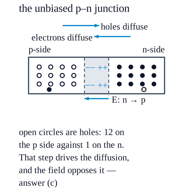 Diffusion is the physical process by which particles move from a region of higher concentration to a region of lower concentration, driven purely by the concentration gradient — it does not require any attractive force or applied potential difference.In an unbiased p-n junction, before any depletion region/barrier field has formed by the diffusion itself, the p-region has a much higher concentration of holes than the n-region (and vice versa for electrons). This concentration gradient is what drives holes to diffuse from p to n (and electrons from n to p). The resulting exposed charges (immobile ions) build up the potential barrier at the junction, and it is this barrier field that subsequently opposes further diffusion (giving a small drift current), not something that causes it. So options (a) and (b) describe effects of the junction field, not the cause of hole diffusion, and (d) is therefore not correct either.Correct statement: (c) hole concentration in p-region is more as compared to n-region.
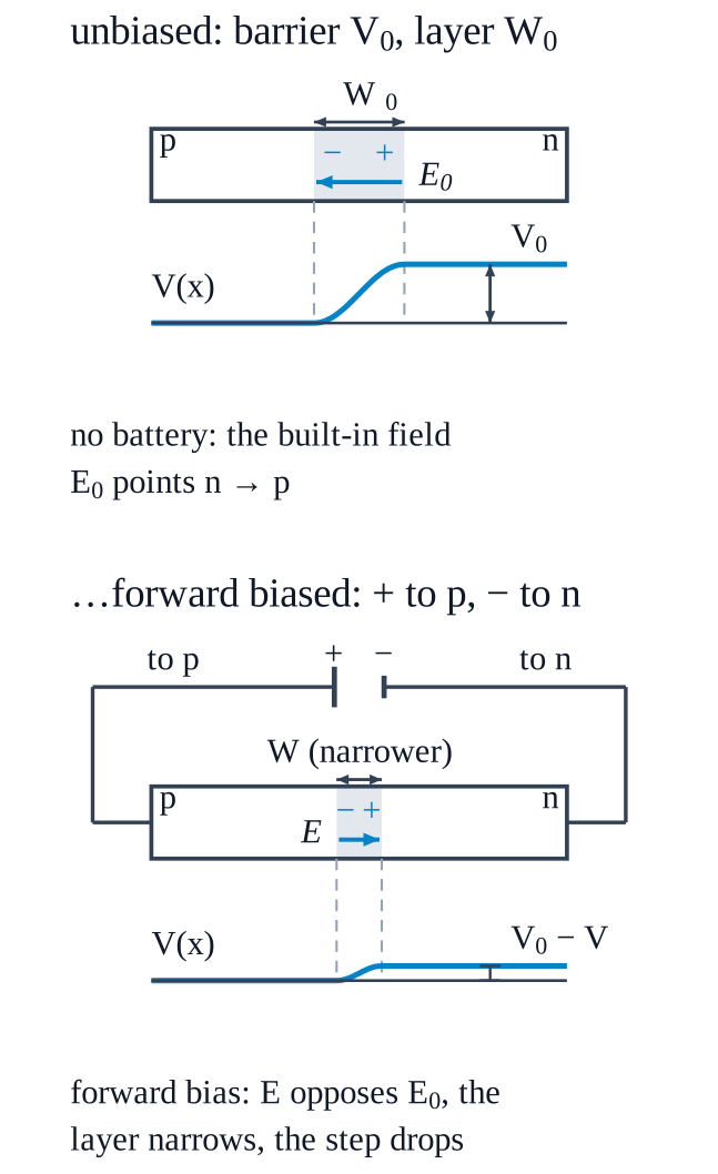 In forward bias, the p-region is connected to the positive terminal and the n-region to the negative terminal of the external battery. The applied electric field is directed opposite to the built-in field of the depletion region, so it partially cancels the internal field.This narrows the depletion region and lowers the potential barrier at the junction (from its equilibrium value, typically by an amount close to the applied voltage for a significant forward bias). With a lowered barrier, majority carriers (holes from p, electrons from n) can cross the junction much more easily, giving a large forward current that increases rapidly with applied voltage — the opposite of raising the barrier or reducing the majority-carrier current to zero.Correct statement: (c) lowers the potential barrier.
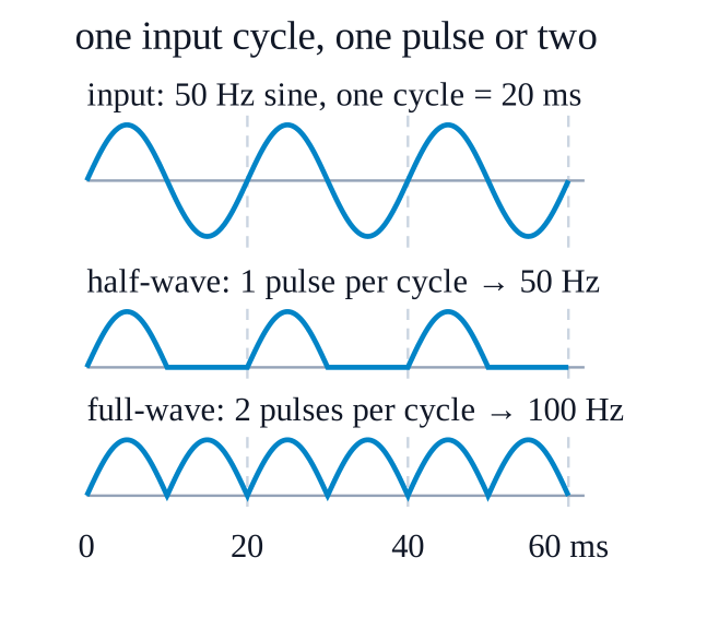 Half-wave rectifier: Only one half-cycle (say, positive) of each input AC cycle is passed to the output; the other half is blocked. So the rectifier produces exactly one output pulse for every one input cycle — the repetition rate of the output pulses equals the input frequency.\[f_{\text{half-wave}} = f_{\text{input}} = 50\ \mathrm{Hz}
\]Full-wave rectifier: Both halves (positive and negative) of each input cycle are converted to output pulses of the same polarity (using a center-tapped transformer or bridge configuration), so two output pulses are produced for every one input cycle.\[f_{\text{full-wave}} = 2f_{\text{input}} = 2 \times 50\ \mathrm{Hz}
\]Half-wave rectifier output frequency = $\displaystyle 50$ Hz; full-wave rectifier output frequency = $\displaystyle 100$ Hz.
Half-wave rectifier: Only one half-cycle (say, positive) of each input AC cycle is passed to the output; the other half is blocked. So the rectifier produces exactly one output pulse for every one input cycle — the repetition rate of the output pulses equals the input frequency.\[f_{\text{half-wave}} = f_{\text{input}} = 50\ \mathrm{Hz}
\]Full-wave rectifier: Both halves (positive and negative) of each input cycle are converted to output pulses of the same polarity (using a center-tapped transformer or bridge configuration), so two output pulses are produced for every one input cycle.\[f_{\text{full-wave}} = 2f_{\text{input}} = 2 \times 50\ \mathrm{Hz}
\]Half-wave rectifier output frequency = $\displaystyle 50$ Hz; full-wave rectifier output frequency = $\displaystyle 100$ Hz.