SolveIt is under development
SolveItClass 12 · Exemplar

NCERT Exemplar · Class 12 Physics Semiconductor Electronics: Materials, Devices and Simple Circuits

40 questions

Multiple Choice Questions (Type II) 9–16 (part 2 of 5)

  1. Exercise 9

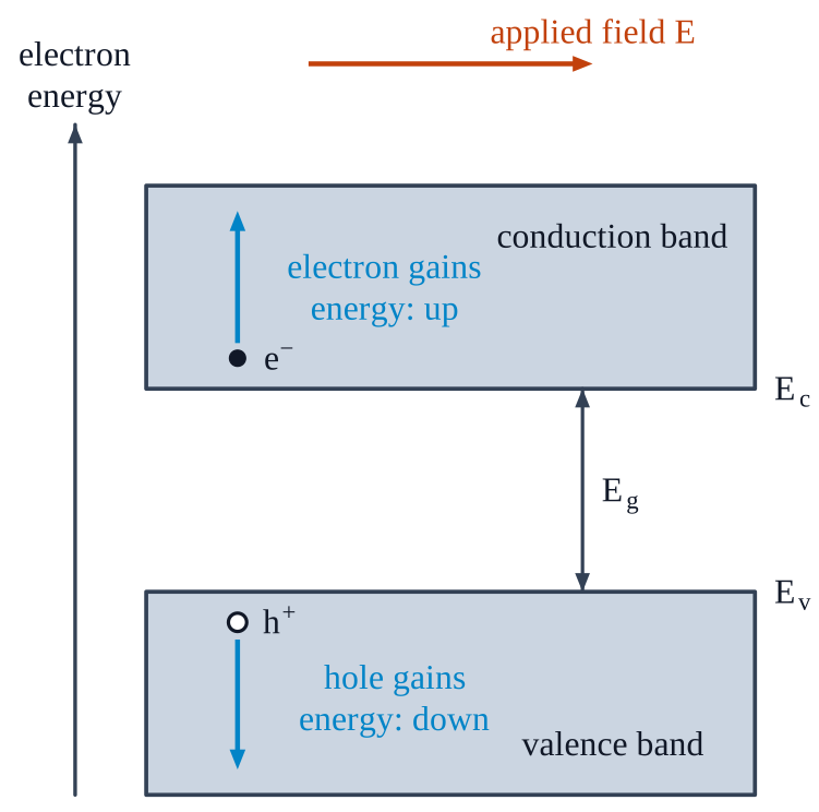
    When an electric field is applied across a semiconductor
    (a)
    electrons move from lower energy level to higher energy level in the conduction band.
    (b)
    electrons move from higher energy level to lower energy level in the conduction band.
    (c)
    holes in the valence band move from higher energy level to lower energy level.
    (d)
    holes in the valence band move from lower energy level to higher energy level.
    NCERT’s answer
    (a), (c)
    (a), (c) The field does work on every carrier, so its kinetic energy rises.\[W=q\,\mathbf{E}\cdot\Delta\mathbf{x}>0 \;\Rightarrow\; KE\uparrow \]\[\text{electron: up the conduction band},\qquad \text{hole: down the valence band} \]NCERT_Solution_Class12_Physics_Exemplar_Ch14_Q9Hole energy is measured downward on the band diagram.
  2. Exercise 10

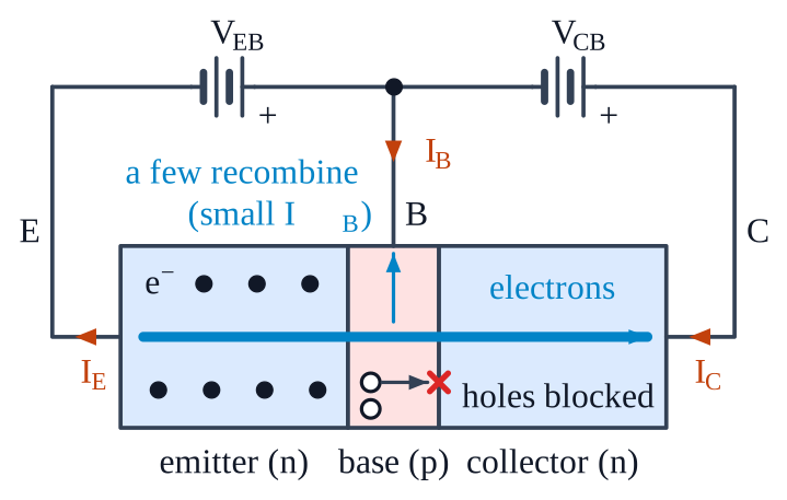
    Consider an npn transitor with its base-emitter junction forward biased and collector base junction reverse biased. Which of the following statements are true?.
    (a)
    Electrons crossover from emitter to collector.
    (b)
    Holes move from base to collector.
    (c)
    Electrons move from emitter to base.
    (d)
    Electrons from emitter move out of base without going to the collector.
    NCERT’s answer
    (a), (c)
    (a), (c) Emitter electrons enter the thin, lightly doped base and nearly all are swept into the collector; only a few recombine, giving the small \(\displaystyle I_B\). Holes cannot cross the reverse-biased collector junction.\[I_E=I_B+I_C,\qquad I_B\ll I_C \]NCERT_Solution_Class12_Physics_Exemplar_Ch14_Q10
  3. Exercise 11

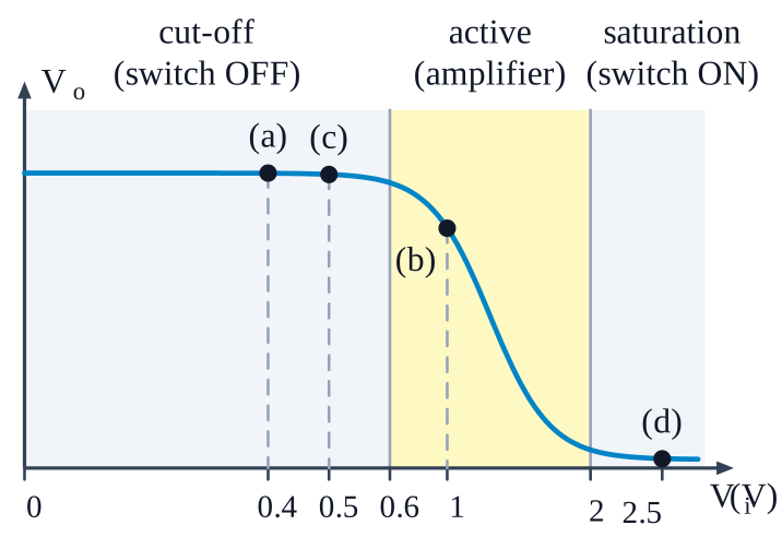
    Figure 14.7\displaystyle 14.7 shows the transfer characteristics of a base biased CE transistor. Which of the following statements are true?
    (a)
    At Vi=0.4 V\displaystyle V_i=0.4 \mathrm{~V}, transistor is in active state.
    (b)
    At Vi=1 V\displaystyle V_i=1 \mathrm{~V}, it can be used as an amplifier.
    (c)
    At Vi=0.5 V\displaystyle V_i=0.5 \mathrm{~V}, it can be used as a switch turned off.
    (d)
    At Vi=2.5 V\displaystyle V_i=2.5 \mathrm{~V}, it can be used as a switch turned on.
    NCERT_Question_Class12_Physics_Exemplar_Ch14_Q11
    NCERT’s answer
    (b), (c), (d)
    (b), (c), (d) Read the regions off the curve: flat \(\displaystyle V_o\) is cut-off, the steep fall is the active region, \(\displaystyle V_o\approx 0\) is saturation.\[V_i=0.4\ \mathrm{V}:\ \text{flat part, cut-off, not active} \]\[V_i=0.5\ \mathrm{V}:\ \text{cut-off}\ \Rightarrow\ \text{switch OFF} \]\[V_i=1\ \mathrm{V}:\ \text{steep part},\ A_V=\frac{\Delta V_o}{\Delta V_i}\ \text{largest}\ \Rightarrow\ \text{amplifier} \]\[V_i=2.5\ \mathrm{V}:\ \text{saturation}\ \Rightarrow\ \text{switch ON} \]NCERT_Solution_Class12_Physics_Exemplar_Ch14_Q11
  4. Exercise 12

    In a npn transistor circuit, the collector current is 10mA. If 95\displaystyle 95 per cent of the electrons emitted reach the collector, which of the following statements are true?
    (a)
    The emitter current will be 8\displaystyle 8 mA.
    (b)
    The emitter current will be 10.53\displaystyle 10.53 mA.
    (c)
    The base current will be 0.53\displaystyle 0.53 mA.
    (d)
    The base current will be 2\displaystyle 2 mA.
    NCERT’s answer
    (b), (c)
    (b), (c) The emitter current is larger than the collector current, and the difference is the base current.\[\alpha=\frac{I_C}{I_E}=0.95 \]\[I_E=\frac{10\ \mathrm{mA}}{0.95}=10.53\ \mathrm{mA} \]\[I_B=I_E-I_C=10.53\ \mathrm{mA}-10\ \mathrm{mA}=0.53\ \mathrm{mA} \]
  5. Exercise 13

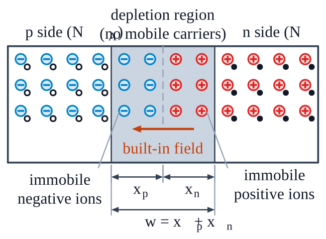
    In the depletion region of a diode
    (a)
    there are no mobile charges
    (b)
    equal number of holes and electrons exist, making the region neutral.
    (c)
    recombination of holes and electrons has taken place.
    (d)
    immobile charged ions exist.
    NCERT’s answer
    (a), (b), (d)
    (a), (b), (d) Only fixed acceptor ions (density \(\displaystyle N_A\)) and donor ions (\(\displaystyle N_D\)) remain, no mobile carriers; their charges are equal and opposite, so the region is neutral overall.NCERT_Solution_Class12_Physics_Exemplar_Ch14_Q13With \(\displaystyle A\) the junction area: \[Q_{\mathrm{net}}=eA\,(N_D x_n-N_A x_p)=0\ \Rightarrow\ N_A x_p=N_D x_n \]
  6. Exercise 14

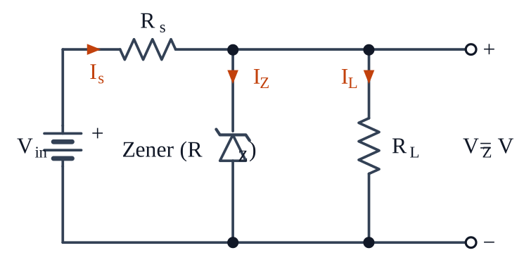
    What happens during regulation action of a Zener diode?
    (a)
    The current in and voltage across the Zenor remains fixed.
    (b)
    The current through the series Resistance (Rs)\displaystyle \left(R_s\right) changes.
    (c)
    The Zener resistance is constant.
    (d)
    The resistance offered by the Zener changes.
    NCERT’s answer
    (b), (d)
    (b), (d) When \(\displaystyle V_{in}\) changes, \(\displaystyle V_Z\) stays nearly fixed but \(\displaystyle I_s\) and \(\displaystyle I_Z\) change, so the Zener's resistance changes.\[I_s=\frac{V_{in}-V_Z}{R_s}=I_Z+I_L,\qquad V_Z\approx\text{const} \]\[V_{in}\uparrow\ \Rightarrow\ I_s\uparrow\ \Rightarrow\ I_Z\uparrow\ \Rightarrow\ R_Z=\frac{V_Z}{I_Z}\downarrow \]NCERT_Solution_Class12_Physics_Exemplar_Ch14_Q14
  7. Exercise 15

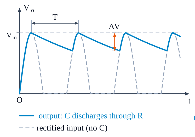
    To reduce the ripples in a rectifier circuit with capacitor filter
    (a)
    RL\displaystyle R_L should be increased.
    (b)
    input frequency should be decreased.
    (c)
    input frequency should be increased.
    (d)
    capacitors with high capacitance should be used.
    NCERT’s answer
    (a), (c), (d)
    (a), (c), (d) The capacitor discharges through \(\displaystyle R_L\) between peaks; less discharge means less ripple.\[\Delta V\approx\frac{I_L\,T}{C},\qquad I_L\approx\frac{V_m}{R_L},\quad T=\frac1f \]\[\Delta V\approx\frac{V_m}{f\,R_L\,C} \]\[R_L\uparrow,\ f\uparrow,\ C\uparrow\ \Rightarrow\ \Delta V\downarrow \]NCERT_Solution_Class12_Physics_Exemplar_Ch14_Q15
  8. Exercise 16

    The breakdown in a reverse biased p–n junction diode is more likely to occur due to
    (a)
    large velocity of the minority charge carriers if the doping concentration is small.
    (b)
    large velocity of the minority charge carriers if the doping concentration is large.
    (c)
    strong electric field in a depletion region if the doping concentration is small.
    (d)
    strong electric field in the depletion region if the doping concentration is large.
    NCERT’s answer
    (a), (d)
    (a), (d) Light doping gives a wide depletion layer: minority carriers gain high speed over a long path and ionise atoms (avalanche). Heavy doping gives a thin layer and a strong field (Zener).\[E\approx\frac{V}{w},\qquad N\uparrow\ \Rightarrow\ w\downarrow\ \Rightarrow\ E\uparrow\ \ (\text{fixed } V) \]