SolveIt is under development
SolveItClass 12 · Exemplar

NCERT Exemplar · Class 12 Physics Semiconductor Electronics: Materials, Devices and Simple Circuits

40 questions

Long Answer Questions 32–40 (part 5 of 5)

  1. Exercise 32

    In the circuit shown in Fig.14.14, when the input voltage of the base resistance is 10V, Vbe\displaystyle \mathrm{V}_{b e} is zero and Vce\displaystyle \mathrm{V}_{\mathrm{ce}} is also zero. Find the values of Ib,Ic\displaystyle I_{\mathrm{b}}, I_{\mathrm{c}} and β\displaystyle \beta. NCERT_Question_Class12_Physics_Exemplar_Ch14_Q32
    NCERT’s answer
    As \(\displaystyle V_{\text {be }}=0\), potential drop across \(\displaystyle R_b\) is 10V. \[\therefore I_b=\frac{10}{400 \times 10^3}=25 \mu \mathrm{~A} \] Since \(\displaystyle \mathrm{V}_{\mathrm{ce}}=0\), potential drop across \(\displaystyle R_c\), i.e. \(\displaystyle I_c R_c\) is 10V. \[\therefore I_c=\frac{10}{3 \times 10^3}=3.33 \times 10^{-3}=3.33 \mathrm{~mA} \text {. } \] \[\therefore \beta=\frac{I_c}{I_b}=\frac{3.33 \times 10^{-3}}{25 \times 10^{-6}}=1.33 \times 10^2=133 . \]
    Emitter is grounded; with \(\displaystyle V_{be}=0\) and \(\displaystyle V_{ce}=0\) the whole $\displaystyle 10$ V falls across \(\displaystyle R_b\) and across \(\displaystyle R_c\).\[I_b=\frac{V_i-V_{be}}{R_b}=\frac{10\ \mathrm{V}-0}{400\times10^{3}\ \Omega}=25\ \mu\mathrm{A} \]\[I_c=\frac{V_{cc}-V_{ce}}{R_c}=\frac{10\ \mathrm{V}-0}{3\times10^{3}\ \Omega}=3.33\ \mathrm{mA} \]\[\beta=\frac{I_c}{I_b}=\frac{3.33\times10^{-3}\ \mathrm{A}}{25\times10^{-6}\ \mathrm{A}}\approx 133 \]Answer: \(\displaystyle I_b=25\ \mu\mathrm{A}\), \(\displaystyle I_c=3.33\ \mathrm{mA}\), \(\displaystyle \beta\approx133\).
  2. Exercise 33

    Draw the output signals C1\displaystyle C_1 and C2\displaystyle C_2 in the given combination of gates (Fig. 14.15\displaystyle 14.15). NCERT_Question_Class12_Physics_Exemplar_Ch14_Q33 NCERT_Question_Class12_Physics_Exemplar_Ch14_Q33_2
    NCERT’s answer
    NCERT_Solution_Class12_Physics_Exemplar_Ch14_Q33_ncert
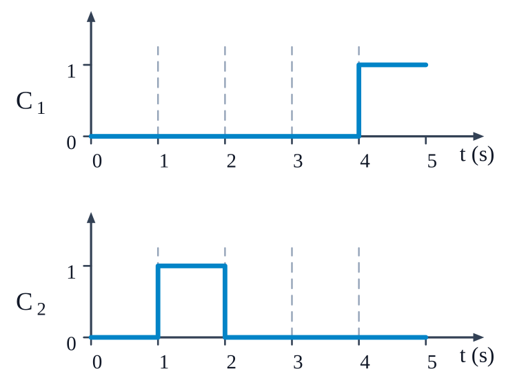
    Gates with tied inputs act as NOT.\[C_1:\quad \overline{A\cdot A}=\bar A,\qquad \overline{B\cdot B}=\bar B,\qquad \overline{\bar A\cdot\bar B}=A+B \]\[C_1=\overline{A+B}\quad(\text{NOR}) \]\[C_2:\quad \overline{A+A}=\bar A,\qquad \overline{B+B}=\bar B,\qquad \overline{\bar A+\bar B}=A\cdot B \]\[C_2=A\cdot B\quad(\text{AND}) \]\[\begin{array}{c|ccccc} t\ (\mathrm{s}) & 0\text{–}1 & 1\text{–}2 & 2\text{–}3 & 3\text{–}4 & 4\text{–}5\\ \hline A & 1 & 1 & 0 & 1 & 0\\ B & 0 & 1 & 1 & 0 & 0\\ C_1 & 0 & 0 & 0 & 0 & 1\\ C_2 & 0 & 1 & 0 & 0 & 0 \end{array} \]NCERT_Solution_Class12_Physics_Exemplar_Ch14_Q33Answer: \(\displaystyle C_1\) is high only for $\displaystyle 4$–$\displaystyle 5$ s; \(\displaystyle C_2\) is high only for $\displaystyle 1$–$\displaystyle 2$ s.
  3. Exercise 34

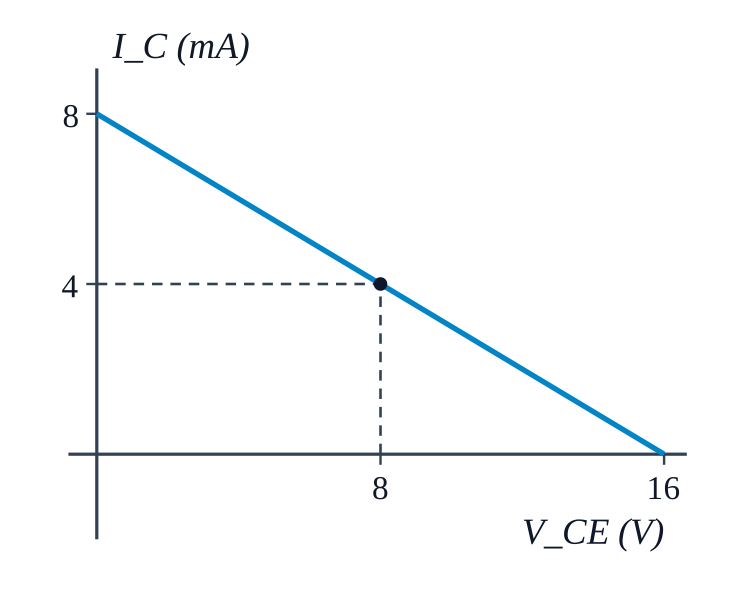
    Consider the circuit arrangement shown in Fig 14.16\displaystyle 14.16 (a) for studying input and output characteristics of npn transistor in CE configuration.Select the values of RB\displaystyle R_B and RC\displaystyle R_C for a transistor whose VBE=0.7 V\displaystyle V_{B E}=0.7 \mathrm{~V}, so that the transistor is operating at point Q as shown in the characteristics shown in Fig. 14.16\displaystyle 14.16 (b).Given that the input impedance of the transistor is very small and VCC=VBB=16 V\displaystyle V_{C C}=V_{B B}=16 \mathrm{~V}, also find the voltage gain and power gain of circuit making appropriate assumptions. NCERT_Question_Class12_Physics_Exemplar_Ch14_Q34 NCERT_Question_Class12_Physics_Exemplar_Ch14_Q34_2
    NCERT’s answer
    From the output characteristics at point \(\displaystyle Q, V_{C E}=8 \mathrm{~V} \& I_C=4 \mathrm{~mA}\) \[\begin{aligned} & V_{C C}=I_C R C+V_{C E} \\ & R_c=\frac{V_{C C}-V_{C E}}{I_C} \\ & R_c=\frac{16-8}{4 \times 10^{-3}}=2 \mathrm{~K} \Omega \end{aligned} \] Since, \[\begin{aligned} & V_{B B}=I_B R_B+V_{B E} \\ & R_B=\frac{16-0.7}{30 \times 10^{-6}}=510 \mathrm{~K} \Omega \end{aligned} \] Now, \(\displaystyle \beta=\frac{I_C}{I_B}=\frac{4 \times 10^{-3}}{30 \times 10^{-6}}=133\) Voltage gain \(\displaystyle =A_V=-\beta \frac{R_C}{R_B}\) \[\begin{aligned} & =-133 \times \frac{2 \times 10^3}{510 \times 10^3} \\ & =0.52 \end{aligned} \] Power Gain \(\displaystyle =A_p=\beta \times A_V\) \[\begin{aligned} & =-\beta^2 \frac{R_C}{R_B} \\ & =(133)^2 \times \frac{2 \times 10^3}{510 \times 10^3}=69 \end{aligned} \]
    At Q: \(\displaystyle I_C=4\ \mathrm{mA}\), \(\displaystyle I_B=30\ \mu\mathrm{A}\), \(\displaystyle V_{CE}=8\ \mathrm{V}\).\[V_{BB}=I_BR_B+V_{BE}\ \Rightarrow\ R_B=\frac{V_{BB}-V_{BE}}{I_B}=\frac{16-0.7}{30\times10^{-6}}\ \Omega=510\ \mathrm{k\Omega} \]\[V_{CC}=V_{CE}+I_CR_C\ \Rightarrow\ R_C=\frac{V_{CC}-V_{CE}}{I_C}=\frac{16-8}{4\times10^{-3}}\ \Omega=2\ \mathrm{k\Omega} \]NCERT_Solution_Class12_Physics_Exemplar_Ch14_Q34Assume the ac gain equals the dc gain, and the transistor's own input resistance is negligible, so the input resistance is \(\displaystyle R_B\).\[\beta=\frac{I_C}{I_B}=\frac{4\ \mathrm{mA}}{30\ \mu\mathrm{A}}=133.3 \]\[A_V=-\beta\,\frac{R_C}{R_B}=-133.3\times\frac{2\ \mathrm{k\Omega}}{510\ \mathrm{k\Omega}}\approx-0.52 \]The minus sign is the $\displaystyle 180$° phase reversal of the CE stage; the magnitude is 0.52.\[A_P=\beta\,|A_V|=133.3\times0.52\approx69 \]Answer: \(\displaystyle R_B=510\ \mathrm{k\Omega}\), \(\displaystyle R_C=2\ \mathrm{k\Omega}\), \(\displaystyle A_V\approx-0.52\) (magnitude $\displaystyle 0.52$), \(\displaystyle A_P\approx69\).
  4. Exercise 35

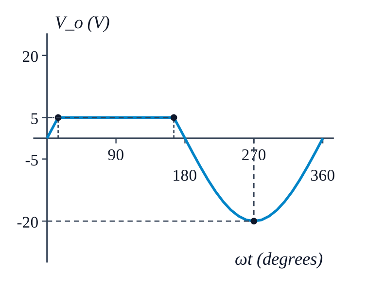
    Assuming the ideal diode, draw the output waveform for the circuit given in Fig. 14.17. Explain the waveform. NCERT_Question_Class12_Physics_Exemplar_Ch14_Q35
    NCERT’s answer
    When input voltage is greater than 5V, diode is conducting When input is less than 5V, diode is open circuit NCERT_Solution_Class12_Physics_Exemplar_Ch14_Q35_ncert
    The diode conducts only when \(\displaystyle V_i\) exceeds the battery's $\displaystyle 5$ V, not when \(\displaystyle V_i>0\).\[V_i>5\ \mathrm{V}:\ \text{diode ON}\ \Rightarrow\ V_o=5\ \mathrm{V} \]\[V_i\le5\ \mathrm{V}:\ \text{diode OFF},\ I=0\ \Rightarrow\ V_o=V_i \]\[20\sin\omega t=5\ \mathrm{V}\ \Rightarrow\ \sin\omega t=0.25\ \Rightarrow\ \omega t=14.5^\circ,\ 165.5^\circ \]NCERT_Solution_Class12_Physics_Exemplar_Ch14_Q35From \(\displaystyle 14.5^\circ\) to \(\displaystyle 165.5^\circ\) the diode conducts and the excess \(\displaystyle V_i-5\) drops across the series resistor. Elsewhere, including the whole negative half-cycle, the output follows the input down to \(\displaystyle -20\ \mathrm{V}\).Answer: The output is the input sine wave with its top clipped flat at \(\displaystyle +5\ \mathrm{V}\) (positive clipper); it swings from \(\displaystyle -20\ \mathrm{V}\) to \(\displaystyle +5\ \mathrm{V}\).
  5. Exercise 36

    Suppose a 'n'-type wafer is created by doping Si crystal having 5×1028\displaystyle 5 \times 10^{28} atoms /m3\displaystyle / \mathrm{m}^3 with 1ppm concentration of As. On the surface 200\displaystyle 200 ppm Boron is added to create 'P' region in this wafer. Considering ni=1.5×10¹⁶ m−3\displaystyle n_i=1.5 \times 10^{16} \mathrm{~m}^{-3}, (i) Calculate the densities of the charge carriers in the n\displaystyle n & p\displaystyle p regions. (ii) Comment which charge carriers would contribute largely for the reverse saturation current when diode is reverse biased.
    NCERT’s answer
    (i)
    In '\(\displaystyle n\)' region; number of \(\displaystyle e^{-}\) is due to As:
    \[\begin{aligned} & n_e=N_D=1 \times 10^{-6} \times 5 \times 10^{28} \text { atoms } / \mathrm{m}^3 \\ & n_e=5 \times 10^{22} / \mathrm{m}^3 \end{aligned} \]
    The minority carriers (hole) is
    \[\begin{aligned} & n_h=\frac{n_i^2}{n_e}=\frac{\left(1.5 \times 10^{16}\right)^2}{5 \times 10^{22}}=\frac{2.25 \times 10^{32}}{5 \times 10^{22}} \\ & n_h=0.45 \times 10 / \mathrm{m}^3 \end{aligned} \]
    Similarly, when Boron is implanted a 'p' type is created with holes
    \[\begin{aligned} & n_h=\mathrm{N}_{\mathrm{A}}=200 \times 10^{-6} \times 5 \times 10^{28} \\ & =1 \times 10^{25} / \mathrm{m}^3 \end{aligned} \]
    This is far greater than \(\displaystyle e^{-}\) that existed in 'n' type wafer on which Boron was diffused.
    Therefore, minority carriers in created 'p' region
    \[\begin{array}{r} n_e=\frac{n_i^2}{n_h}=\frac{2.25 \times 10^{32}}{1 \times 10^{25}} \\ =2.25 \times 10^7 / \mathrm{m}^3 \end{array} \]
    (ii)
    Thus, when reverse biased \(\displaystyle 0.45 \times 10^{10} / \mathrm{m}^3\), holes of '\(\displaystyle n\)' region would contribute more to the reverse saturation current than \(\displaystyle 2.25 \times 10^7 / \mathrm{m}^3\) minority \(\displaystyle \mathrm{e}^{-}\) of p type region.
    n-region (As donors):
    \[N_D=5\times10^{28}\times10^{-6}=5\times10^{22}\ \mathrm{m^{-3}}\ \Rightarrow\ n_e\approx N_D=5\times10^{22}\ \mathrm{m^{-3}} \]
    \[n_h=\frac{n_i^{2}}{n_e}=\frac{(1.5\times10^{16})^{2}}{5\times10^{22}}=4.5\times10^{9}\ \mathrm{m^{-3}} \]
    p-region (B acceptors far exceed the donors):
    \[N_A=5\times10^{28}\times200\times10^{-6}=10^{25}\ \mathrm{m^{-3}}\ \Rightarrow\ n_h\approx N_A-N_D\approx10^{25}\ \mathrm{m^{-3}} \]
    \[n_e=\frac{n_i^{2}}{n_h}=\frac{2.25\times10^{32}}{10^{25}}=2.25\times10^{7}\ \mathrm{m^{-3}} \]
    (ii)
    Reverse saturation current is carried by minority carriers:
    \[\frac{n_h\ (\text{n-region})}{n_e\ (\text{p-region})}=\frac{4.5\times10^{9}}{2.25\times10^{7}}=200 \]
    Answer: n-region: \(\displaystyle n_e=5\times10^{22}\), \(\displaystyle n_h=4.5\times10^{9}\ \mathrm{m^{-3}}\); p-region: \(\displaystyle n_h\approx10^{25}\), \(\displaystyle n_e=2.25\times10^{7}\ \mathrm{m^{-3}}\). Holes (minority carriers of the n-region) contribute largely to the reverse saturation current.
  6. Exercise 37

    An X-OR gate has following truth table:
    ABY
    0\displaystyle 00\displaystyle 00\displaystyle 0
    0\displaystyle 01\displaystyle 11\displaystyle 1
    1\displaystyle 10\displaystyle 01\displaystyle 1
    1\displaystyle 11\displaystyle 10\displaystyle 0
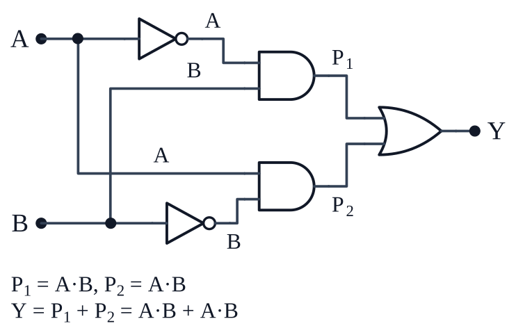
    It is represented by following logic relation Y=A‾.B+A.B‾\mathrm{Y}=\overline{\mathrm{A}} . \mathrm{B}+\mathrm{A} . \overline{\mathrm{B}} Build this gate using AND, OR and NOT gates.
    Two NOT gates give \(\displaystyle \overline{A}\) and \(\displaystyle \overline{B}\); two AND gates form the product terms; one OR gate adds them.\[\overline{A}=\mathrm{NOT}(A),\qquad \overline{B}=\mathrm{NOT}(B) \]\[P_1=\overline{A}\cdot B\ \ (\mathrm{AND}),\qquad P_2=A\cdot\overline{B}\ \ (\mathrm{AND}) \]\[Y=P_1+P_2\ \ (\mathrm{OR}) \]NCERT_Solution_Class12_Physics_Exemplar_Ch14_Q37Caution: split each input into two branches, so that \(\displaystyle A\) reaches its own AND gate directly and the other one through NOT (likewise \(\displaystyle B\)). Check:\[(A,B)=(0,0):\ \ 1\cdot 0+0\cdot 1=0 \]\[(A,B)=(0,1):\ \ 1\cdot 1+0\cdot 0=1 \]\[(A,B)=(1,0):\ \ 0\cdot 0+1\cdot 1=1 \]\[(A,B)=(1,1):\ \ 0\cdot 1+1\cdot 0=0 \]Answer: \(\displaystyle Y=\overline{A}\,B+A\,\overline{B}\), built from $\displaystyle 2$ NOT, $\displaystyle 2$ AND and $\displaystyle 1$ OR gate wired as in the figure.
  7. Exercise 38

    Consider a box with three terminals on top of it as shown in Fig.14.18 (a):
    Three components namely, two germanium diodes and one resistor are connected across these three terminals in some arrangement.
    A student performs an experiment in which any two of these three terminals are connected in the circuit shown in Fig. 14.18\displaystyle 14.18 (b).
    The student obtains graphs of current-voltage characteristics for unknown combination of components between the two terminals connected in the circuit.
    The graphs are
    (i)
    when A is positive and B is negative
    (ii)
    when A is negative and B is positive
    (iii)
    When B is negative and C is positive
    (iv)
    When B is positive and C is negative
    (v)
    When A is positive and C is negative
    (vi)
    When A is negative and C is positive
    From these graphs of current - voltage characteristic shown in Fig. 14.18\displaystyle 14.18 (c) to (h), determine the arrangement of components between A, B and C.
    NCERT_Question_Class12_Physics_Exemplar_Ch14_Q38
    NCERT_Question_Class12_Physics_Exemplar_Ch14_Q38_2
    NCERT_Question_Class12_Physics_Exemplar_Ch14_Q38_3
    NCERT_Question_Class12_Physics_Exemplar_Ch14_Q38_4
    NCERT_Question_Class12_Physics_Exemplar_Ch14_Q38_5
    NCERT_Question_Class12_Physics_Exemplar_Ch14_Q38_6
    NCERT_Question_Class12_Physics_Exemplar_Ch14_Q38_7
    NCERT_Question_Class12_Physics_Exemplar_Ch14_Q38_8
    NCERT’s answer
    NCERT_Solution_Class12_Physics_Exemplar_Ch14_Q38_ncert
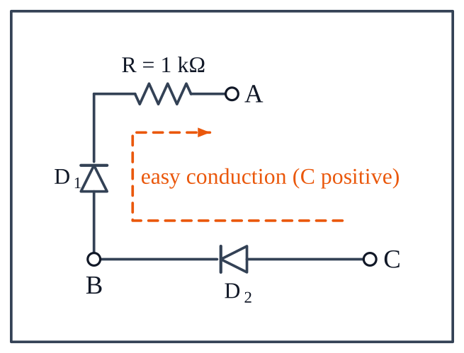
    Pair by pair: one polarity conducts, the other blocks.\[A^{-}B^{+}:\ V_{\mathrm{th}}=0.7\ \mathrm{V},\ \ \frac{1}{\text{slope}}=1000\ \Omega;\qquad A^{+}B^{-}:\ I\approx 0 \]\[\Rightarrow\ \text{A–B: diode } D_1\ (B\to A)\ \text{in series with } R=1\ \mathrm{k\Omega} \]\[C^{+}B^{-}:\ V_{\mathrm{th}}=0.7\ \mathrm{V},\ \text{steep rise};\qquad B^{+}C^{-}:\ I\approx 0 \]\[\Rightarrow\ \text{B–C: one diode } D_2\ (C\to B) \text{ alone} \]\[C^{+}A^{-}:\ V_{\mathrm{th}}=1.4\ \mathrm{V}=0.7\ \mathrm{V}+0.7\ \mathrm{V};\qquad A^{+}C^{-}:\ I\approx 0 \]\[\Rightarrow\ \text{A–C: } D_2,\ D_1,\ R \text{ in series, both diodes pointing } C\to A \]NCERT_Solution_Class12_Physics_Exemplar_Ch14_Q38Caution: a resistor in parallel with a diode would also pass \(\displaystyle V/1\,\mathrm{k\Omega}\) in the blocking polarity. The blocking graphs show almost no current, so nothing is in parallel.Answer: \(\displaystyle C\to D_2\to B\to D_1\to R\to A\) in series, with \(\displaystyle R=1\ \mathrm{k\Omega}\).
  8. Exercise 39

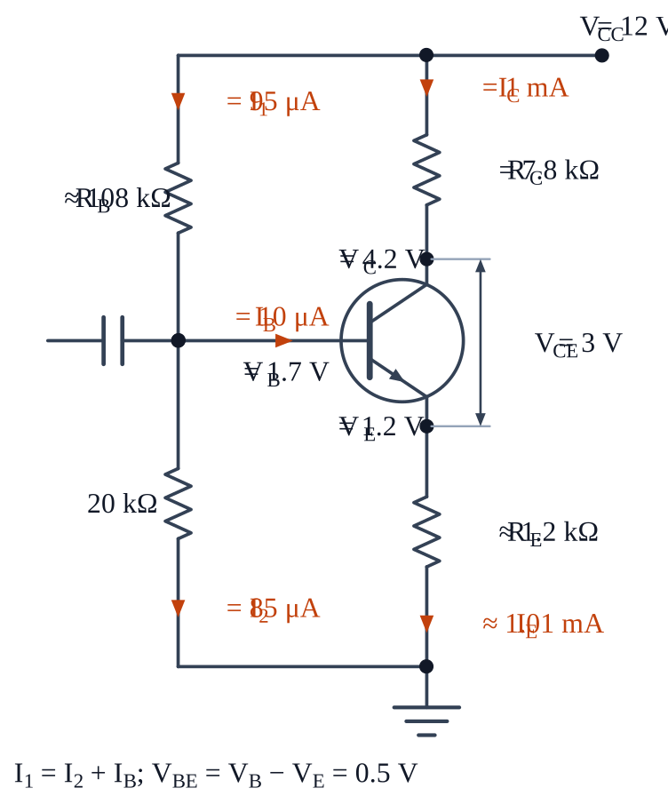
    For the transistor circuit shown in Fig.14.19, evaluate VE,RB,RE\displaystyle V_E, R_B, R_E given IC=1 mA,VCE=3 V,VBE=0.5 V\displaystyle I_C=1 \mathrm{~mA}, V_{C E}=3 \mathrm{~V}, V_{B E}=0.5 \mathrm{~V} and VCC=12 V\displaystyle V_{C C}=12 \mathrm{~V}, β=100\displaystyle \beta=100. NCERT_Question_Class12_Physics_Exemplar_Ch14_Q39
    NCERT’s answer
    \(\displaystyle I_C \approx I_E \therefore I_C\left(R_C+R_E\right)+\mathrm{V}_{\mathrm{CE}}=12 \mathrm{~V}\) \[R_E=9-\mathrm{R}_{\mathrm{C}}=1.2 \mathrm{~K} \Omega \] \[\begin{aligned} & \therefore V_E=1.2 \mathrm{~V} \\ & V_B=V_E+V_{B E}=1.7 \mathrm{~V} \\ & I=\frac{V_B}{20 \mathrm{~K}}=0.085 \mathrm{~mA} \end{aligned} \] \[R_B=\frac{12-1.7}{I_C / \beta+0.085}=\frac{10.3}{0.01+1.085}=108 \mathrm{~K} \Omega \]
    \[V_C = V_{CC}-I_C R_C = 12-(1\ \mathrm{mA})(7.8\ \mathrm{k\Omega}) = 4.2\ \mathrm{V} \]\[V_E = V_C - V_{CE} = 4.2-3 = 1.2\ \mathrm{V} \]\[I_B=\frac{I_C}{\beta}=\frac{1\ \mathrm{mA}}{100}=10\ \mu\mathrm{A},\qquad I_E=I_C+I_B\approx 1.01\ \mathrm{mA} \]\[R_E=\frac{V_E}{I_E}=\frac{1.2\ \mathrm{V}}{1.01\ \mathrm{mA}}\approx 1.19\ \mathrm{k\Omega}\approx 1.2\ \mathrm{k\Omega} \]Base bias chain:NCERT_Solution_Class12_Physics_Exemplar_Ch14_Q39\[V_B=V_E+V_{BE}=1.2+0.5=1.7\ \mathrm{V} \]\[I_2=\frac{V_B}{20\ \mathrm{k\Omega}}=\frac{1.7\ \mathrm{V}}{20\ \mathrm{k\Omega}}=85\ \mu\mathrm{A} \]Caution: \(\displaystyle R_B\) carries the divider current plus the base current.\[I_1=I_2+I_B=85+10=95\ \mu\mathrm{A} \]\[R_B=\frac{V_{CC}-V_B}{I_1}=\frac{12-1.7}{95\times 10^{-6}\ \mathrm{A}}\approx 1.08\times 10^{5}\ \Omega\approx 108\ \mathrm{k\Omega} \]Answer: \(\displaystyle V_E=1.2\ \mathrm{V}\), \(\displaystyle R_E\approx 1.2\ \mathrm{k\Omega}\), \(\displaystyle R_B\approx 108\ \mathrm{k\Omega}\).
  9. Exercise 40

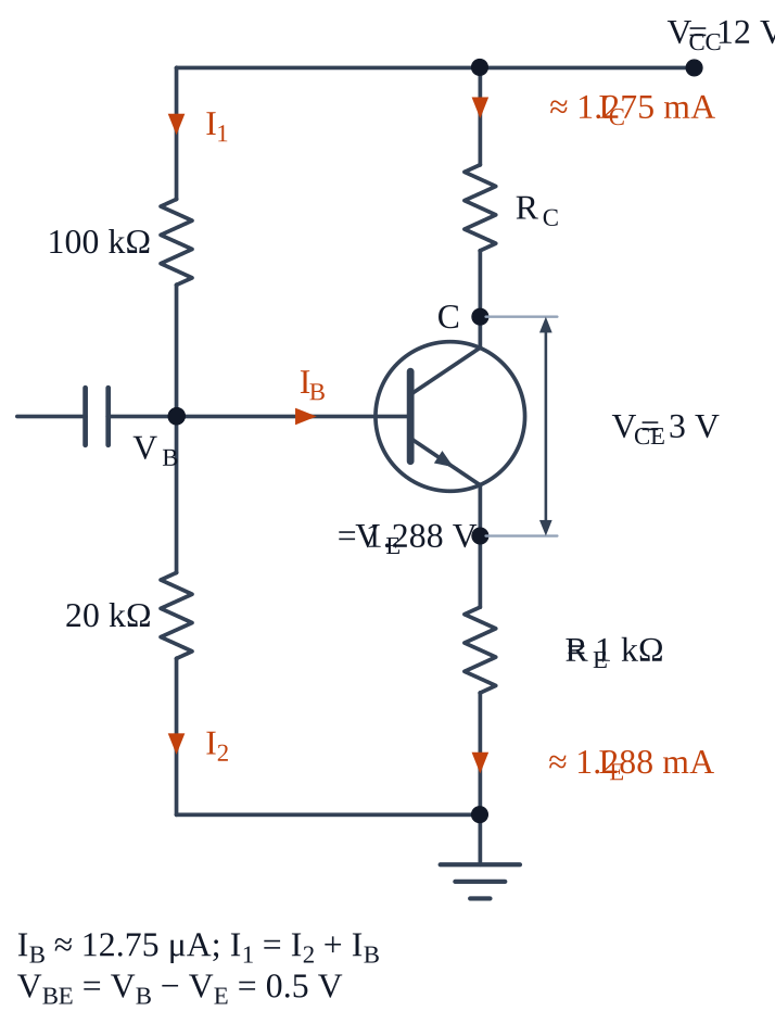
    In the circuit shown in Fig.14.20, find the value of RC\displaystyle R_C. NCERT_Question_Class12_Physics_Exemplar_Ch14_Q40
    The figure prints no value for the emitter resistor; \(\displaystyle R_E = 1\ \mathrm{k\Omega}\) is the value NCERT's answer uses.\[V_{CC} = 12\ \mathrm{V},\quad \beta = 100,\quad V_{BE} = 0.5\ \mathrm{V},\quad V_{CE} = 3\ \mathrm{V},\quad R_E = 1\ \mathrm{k\Omega} \]NCERT_Solution_Class12_Physics_Exemplar_Ch14_Q40Emitter side:\[I_E = I_B + I_C = (\beta + 1)\,I_B = 101\,I_B \]\[V_B = V_{BE} + I_E R_E = 0.5\ \mathrm{V} + (101\,I_B)(1\ \mathrm{k\Omega}) = 0.5\ \mathrm{V} + (101\ \mathrm{k\Omega})\,I_B \]Caution: the \(\displaystyle 100\ \mathrm{k\Omega}\) resistor carries the \(\displaystyle 20\ \mathrm{k\Omega}\) current plus the base current.\[I_1 = I_2 + I_B,\qquad I_2 = \frac{V_B}{20\ \mathrm{k\Omega}} \]\[V_{CC} - V_B = I_1\,(100\ \mathrm{k\Omega}) = \left(\frac{V_B}{20\ \mathrm{k\Omega}} + I_B\right)(100\ \mathrm{k\Omega}) \]\[12\ \mathrm{V} - V_B = 5\,V_B + (100\ \mathrm{k\Omega})\,I_B \;\Rightarrow\; 12\ \mathrm{V} = 6\,V_B + (100\ \mathrm{k\Omega})\,I_B \]Put in \(\displaystyle V_B\):\[12\ \mathrm{V} = 3\ \mathrm{V} + (606\ \mathrm{k\Omega})\,I_B + (100\ \mathrm{k\Omega})\,I_B = 3\ \mathrm{V} + (706\ \mathrm{k\Omega})\,I_B \]\[I_B = \frac{9\ \mathrm{V}}{706\ \mathrm{k\Omega}} \approx 12.75\ \mu\mathrm{A} \]\[I_C = \beta I_B = 100 \times 12.75\ \mu\mathrm{A} \approx 1.275\ \mathrm{mA} \]\[I_E = 101\,I_B = 101 \times 12.75\ \mu\mathrm{A} \approx 1.288\ \mathrm{mA} \]\[V_E = I_E R_E = (1.288\ \mathrm{mA})(1\ \mathrm{k\Omega}) = 1.288\ \mathrm{V} \]Collector loop:\[V_{CC} = I_C R_C + V_{CE} + V_E \]\[R_C = \frac{V_{CC} - V_{CE} - V_E}{I_C} = \frac{12\ \mathrm{V} - 3\ \mathrm{V} - 1.288\ \mathrm{V}}{1.275\ \mathrm{mA}} = \frac{7.712\ \mathrm{V}}{1.275\ \mathrm{mA}} \approx 6.05\ \mathrm{k\Omega} \]Answer: \(\displaystyle R_C \approx 6.05\ \mathrm{k\Omega}\) (about \(\displaystyle 6\ \mathrm{k\Omega}\)), with \(\displaystyle R_E = 1\ \mathrm{k\Omega}\).NCERT prints: \(\displaystyle R_C \approx 0.56\ \mathrm{k\Omega}\) -- its base-loop equation leaves out the \(\displaystyle 20\ \mathrm{k\Omega}\) resistor of the drawn divider.