SolveIt is under development
SolveItClass 12 · Exemplar

NCERT Exemplar · Class 12 Physics Semiconductor Electronics: Materials, Devices and Simple Circuits

40 questions

Multiple Choice Questions (Type I) 1–8 (part 1 of 5)

  1. Exercise 1

    The conductivity of a semiconductor increases with increase in temperature because
    (a)
    number density of free current carriers increases.
    (b)
    relaxation time increases.
    (c)
    both number density of carriers and relaxation time increase.
    (d)
    number density of current carriers increases, relaxation time decreases but effect of decrease in relaxation time is much less than increase in number density.
    NCERT’s answer
    (d)
    (d) Carrier density rises sharply with temperature; relaxation time falls only slightly, so conductivity rises.\[\sigma=\frac{n e^{2}\tau}{m} \]\[T\uparrow \Rightarrow n\uparrow\ \text{(more bonds break)},\qquad \tau\downarrow\ \text{(more lattice collisions)} \]\[\frac{\Delta n}{n}\gg\frac{\lvert\Delta\tau\rvert}{\tau} \Rightarrow \sigma\uparrow \]
  2. Exercise 2

    In Fig. 14.1\displaystyle 14.1, Vo\displaystyle V_o is the potential barrier across a p-n junction, when no battery is connected across the junction
    (a)
    1\displaystyle 1 and 3\displaystyle 3 both correspond to forward bias of junction
    (b)
    3\displaystyle 3 corresponds to forward bias of junction and 1\displaystyle 1 corresponds to reverse bias of junction
    (c)
    1\displaystyle 1 corresponds to forward bias and 3\displaystyle 3 corresponds to reverse bias of junction.
    (d)
    3\displaystyle 3 and 1\displaystyle 1 both correspond to reverse bias of junction.
    NCERT_Question_Class12_Physics_Exemplar_Ch14_Q2
    NCERT’s answer
    (b)
    (b) Curve $\displaystyle 2$ reaches \(\displaystyle V_0\): no battery. Curve $\displaystyle 3$ is lower (barrier reduced), curve $\displaystyle 1$ is higher (barrier raised).\[V_{3}<V_{0}<V_{1} \]\[\text{forward bias: } V_b=V_0-V<V_0 \Rightarrow \text{curve 3} \]\[\text{reverse bias: } V_b=V_0+V>V_0 \Rightarrow \text{curve 1} \]
  3. Exercise 3

    In Fig. 14.2\displaystyle 14.2, assuming the diodes to be ideal,
    (a)
    D1\displaystyle \mathrm{D}_1 is forward biased and D2\displaystyle \mathrm{D}_2 is reverse biased and hence current flows from A to B
    (b)
    D2\displaystyle \mathrm{D}_2 is forward biased and D1\displaystyle \mathrm{D}_1 is reverse biased and hence no current flows from B to A and vice versa.
    (c)
    D1\displaystyle \mathrm{D}_1 and D2\displaystyle \mathrm{D}_2 are both forward biased and hence current flows from A to B.
    (d)
    D1\displaystyle \mathrm{D}_1 and D2\displaystyle \mathrm{D}_2 are both reverse biased and hence no current flows from A to B and vice versa.
    NCERT_Question_Class12_Physics_Exemplar_Ch14_Q3
    NCERT’s answer
    (b)
    (b) Any current would run from B (higher potential) to A. \(\displaystyle \mathrm{D_2}\) is oriented to pass it, \(\displaystyle \mathrm{D_1}\) to block it, so none flows.\[V_B-V_A=0-(-10\ \mathrm{V})=+10\ \mathrm{V} \Rightarrow \text{current direction } B\to A \]\[\mathrm{D_2}:\ B\to A \text{ is anode}\to\text{cathode} \Rightarrow \text{forward biased} \]\[\mathrm{D_1}:\ B\to A \text{ is cathode}\to\text{anode} \Rightarrow \text{reverse biased},\quad I\approx 0 \]
  4. Exercise 4

    A 220\displaystyle 220 V A.C. supply is connected between points A and B (Fig. 14.3\displaystyle 14.3). What will be the potential difference V\displaystyle V across the capacitor?
    (a)
    220V.
    (b)
    110V.
    (c)
    0V.
    (d)
    2202 V\displaystyle 220 \sqrt{2} \mathrm{~V}.
    NCERT_Question_Class12_Physics_Exemplar_Ch14_Q4
    NCERT’s answer
    (d)
    (d) The diode charges the capacitor to the peak voltage, and the capacitor has no path to discharge. The $\displaystyle 220$ V is r.m.s., so the peak is larger.\[V_0=\sqrt{2}\,V_{rms}=\sqrt{2}\times 220\ \mathrm{V}=220\sqrt{2}\ \mathrm{V}\approx 311\ \mathrm{V} \]\[V=V_0=220\sqrt{2}\ \mathrm{V} \]
  5. Exercise 5

    Hole is
    (a)
    an anti-particle of electron.
    (b)
    a vacancy created when an electron leaves a covalent bond.
    (c)
    absence of free electrons.
    (d)
    an artifically created particle.
    NCERT’s answer
    (b)
    (b) A hole is the vacancy left in a covalent bond when an electron leaves it. It is not a positron, and the missing electron was a bond electron, not a free one.\[\text{bond electron freed} \Rightarrow \text{vacancy} = \text{hole},\qquad \text{effective charge}=+e \]
  6. Exercise 6

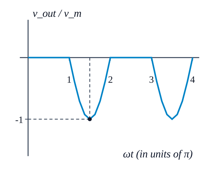
    The output of the given circuit in Fig. 14.4.
    (a)
    would be zero at all times.
    (b)
    would be like a half wave rectifier with positive cycles in output.
    (c)
    would be like a half wave rectifier with negative cycles in output.
    (d)
    would be like that of a full wave rectifier.
    NCERT_Question_Class12_Physics_Exemplar_Ch14_Q6
    NCERT’s answer
    (c)
    (c) On the positive half cycle the diode conducts and shorts the output. On the negative half cycle it blocks, so the source voltage appears at the output.\[v_{in}>0:\ \text{diode forward} \Rightarrow v_{out}\approx 0 \]\[v_{in}<0:\ \text{diode reverse} \Rightarrow I\approx 0,\quad v_{out}=v_{in}-IR=v_m\sin\omega t<0 \]NCERT_Solution_Class12_Physics_Exemplar_Ch14_Q6
  7. Exercise 7

    In the circuit shown in Fig. 14.5\displaystyle 14.5, if the diode forward voltage drop is 0.3\displaystyle 0.3 V, the voltage difference between A and B is
    (a)
    1.3\displaystyle 3 V
    (b)
    2.3\displaystyle 3 V
    (c)
    0\displaystyle 0 (d) 0.5\displaystyle 0.5 V
    NCERT_Question_Class12_Physics_Exemplar_Ch14_Q7
    NCERT’s answer
    (b)
    (b) The capacitor blocks d.c., so the full $\displaystyle 0.2$ mA flows through both resistors and the forward-biased diode.\[V_{AB}=IR_1+V_D+IR_2 \]\[V_{AB}=(0.2\times10^{-3}\ \mathrm{A})(5\times10^{3}\ \Omega)+0.3\ \mathrm{V}+(0.2\times10^{-3}\ \mathrm{A})(5\times10^{3}\ \Omega) \]\[V_{AB}=1\ \mathrm{V}+0.3\ \mathrm{V}+1\ \mathrm{V}=2.3\ \mathrm{V} \]
  8. Exercise 8

    Truth table for the given circuit (Fig. 14.6\displaystyle 14.6) is
    (a)
    ABE
    0\displaystyle 00\displaystyle 01\displaystyle 1
    0\displaystyle 01\displaystyle 10\displaystyle 0
    1\displaystyle 10\displaystyle 01\displaystyle 1
    1\displaystyle 11\displaystyle 10\displaystyle 0
    (b)
    ABE
    0\displaystyle 00\displaystyle 01\displaystyle 1
    0\displaystyle 01\displaystyle 10\displaystyle 0
    1\displaystyle 10\displaystyle 00\displaystyle 0
    1\displaystyle 11\displaystyle 11\displaystyle 1
    (c)
    ABE
    0\displaystyle 00\displaystyle 00\displaystyle 0
    0\displaystyle 01\displaystyle 11\displaystyle 1
    1\displaystyle 10\displaystyle 00\displaystyle 0
    1\displaystyle 11\displaystyle 11\displaystyle 1
    (d)
    ABE
    0\displaystyle 00\displaystyle 00\displaystyle 0
    0\displaystyle 01\displaystyle 11\displaystyle 1
    1\displaystyle 10\displaystyle 01\displaystyle 1
    1\displaystyle 11\displaystyle 10\displaystyle 0
    NCERT_Question_Class12_Physics_Exemplar_Ch14_Q8
    NCERT’s answer
    (c)
    (c) The final gate must be OR; drawn as AND it would give \(\displaystyle E=0\) always, which no table shows.\[C=A\cdot B,\qquad D=\bar{A}\cdot B \]\[E=C+D=AB+\bar{A}B=(A+\bar{A})\,B=B \]\[(A,B)=(0,0),\ (0,1),\ (1,0),\ (1,1)\ \Rightarrow\ E=0,\ 1,\ 0,\ 1 \]