✓ Board-verified
Physics · 2024 · 4 marks
Semiconductor Electronics: Materials, Devices and Simple CircuitsApplication of Junction Diode as a Rectifier4 marksUnderstandcase study
CBSE 2024 · Region 1 · Set 1 · Q30
Junction Diode as a Rectifier: The process of conversion of an ac voltage into a dc voltage is called rectification and the device which performs…
Junction Diode as a Rectifier : The process of conversion of an ac voltage into a dc voltage is called rectification and the device which performs this conversion is called a rectifier. The characteristics of a $\displaystyle \mathrm{p}-\mathrm{n}$ junction diode reveal that when a $\displaystyle \mathrm{p}-\mathrm{n}$ junction diode is forward biased, it offers a low resistance and when it is reverse biased, it offers a high resistance. Hence, a p-n junction diode conducts only when it is forward biased. This property of a $\displaystyle \mathrm{p}-\mathrm{n}$ junction diode makes it suitable for its use as a rectifier. Thus, when an ac voltage is applied across a $\displaystyle \mathrm{p}-\mathrm{n}$ junction, it conducts only during those alternate half cycles for which it is forward biased. A rectifier which rectifies only half cycle of an ac voltage is called a half-wave rectifier and one that rectifies both the half cycles is known as a full-wave rectifier.
(i)
The root mean square value of an alternating voltage applied to a full-wave rectifier is $\displaystyle \frac{\mathrm{V}_{0}}{\sqrt{2}}$. Then the root mean square value of the rectified output voltage is :
(A)
$\displaystyle \frac{\mathrm{V}_{0}}{\sqrt{2}}$
(B)
$\displaystyle \frac{\mathrm{V}_{0}^{2}}{\sqrt{2}}$
(C)
$\displaystyle \frac{2 \mathrm{~V}_{0}}{\sqrt{2}}$
(D)
$\displaystyle \frac{\mathrm{V}_{0}}{2 \sqrt{2}}$
(ii)
In a full-wave rectifier, the current in each of the diodes flows for :
(A)
Complete cycle of the input signal
(B)
Half cycle of the input signal
(C)
Less than half cycle of the input signal
(D)
Only for the positive half cycle of the input signal
(iii)
In a full-wave rectifier :
(A)
Both diodes are forward biased at the same time.
(B)
Both diodes are reverse biased at the same time.
(C)
One is forward biased and the other is reverse biased at the same time.
(D)
Both are forward biased in the first half of the cycle and reverse biased in the second half of the cycle.
(iv)
An alternating voltage of frequency of $\displaystyle 50$ Hz is applied to a half-wave rectifier. Then the ripple frequency of the output will be :
(A)
$\displaystyle 100$ Hz
(B)
$\displaystyle 50$ Hz
(C)
$\displaystyle 25$ Hz
(D)
$\displaystyle 150$ Hz
A signal, as shown in the figure, is applied to a p-n junction diode. Identify the output across resistance $\displaystyle \mathrm{R}_{\mathrm{L}}$ : 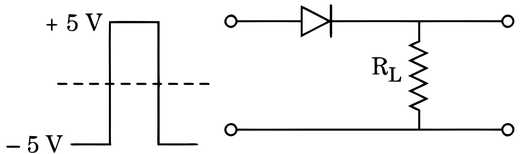 (A)
(A) 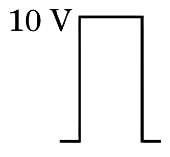 (B)
(B) 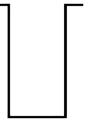 (C)
(C) 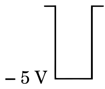 (D)
(D) 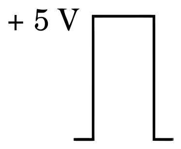
(A) (B) (C) (D) Marking-scheme solution
(i) (A) \(\displaystyle \frac{\mathrm{V} o}{\sqrt{2}}\)
(ii) (B) half cycle of the input signal
(iii) (C) One is forward biased and the other is reverse biased at the
same time(iv) a) (B) $\displaystyle 50$ Hz
OR
b) (D) \(\displaystyle \begin{aligned} & +5 \mathrm{~V} \\ & \end{aligned}\)
All Semiconductor Electronics: Materials, Devices and Simple Circuits questions2024 question paperNCERT solutions: Semiconductor Electronics: Materials, Devices and Simple CircuitsPractice Semiconductor Electronics: Materials, Devices and Simple Circuits →
More from Semiconductor Electronics: Materials, Devices and Simple Circuits
- With the help of a circuit diagram, explain the working of a p-n junction diode as a full-wave rectifier. Also draw its input and output waveforms.2022 · asked 2×
- State the working principle of an LED. Write any two important advantages and two disadvantages of LED.2022
- What are majority and minority charge carriers in an extrinsic semiconductor? A p-n junction is forward biased. Describe the movement of the charge…2025
- Draw the circuit diagrams for obtaining the V-I characteristics of a p-n junction diode. Explain briefly the salient features of the V - I…2024
- A pure Si crystal having 5 × 10^28 atoms m^-3 is dopped with 1 ppm concentration of antimony. If the concentration of holes in the doped crystal is…2024
- With the help of circuit diagrams, briefly explain the forward biasing and the reverse biasing of a p-n junction diode.2026
- In an intrinsic semiconductor, carrier's concentration is 5 × 10^8 m^-3. On doping with impurity atoms, the hole concentration becomes 8 × 10^12…2025
- Assertion: A hole is an apparent free particle with effective positive electronic charge. Reason ( R ): A hole is not necessarily a vacancy left…2025
CBSE Class 12 Physics past-paper question from the 2024 board exam, with the answer as CBSE’s own marking scheme gives it. Where our answers come from.