✓ Board-verified
Physics · 2024 · 3 marks
Semiconductor Electronics: Materials, Devices and Simple CircuitsClassification of Metals, Conductors and Semiconductors3 marksUnderstandshort answer
CBSE 2024 · Region 3 · Set 2 · Q28
(a) Draw the circuit diagrams for obtaining the V - I characteristics of a p-n junction diode. Explain briefly the salient features of the V - I…
(a)
Draw the circuit diagrams for obtaining the $\displaystyle \mathrm{V}-\mathrm{I}$ characteristics of a p-n junction diode. Explain briefly the salient features of the V - I characteristics in (i) forward biasing, and (ii) reverse biasing.
OR
(b)
On the basis of energy band diagrams, distinguish between (i) an insulator, (ii) a semiconductor, and (iii) a conductor.
Marking-scheme solution
(a)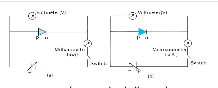
Salient features
(i)
Forward biasing - After threshold voltage or cut in voltage diode current increase significantly (exponentially), even for a small increase in the diode bias voltage.
(ii)
Reverse biasing - Current is very small ($\displaystyle \sim\mu\mathrm{A}$) and almost remains constant and it increases rapidly after breakdown voltage.
OR(b) (i) 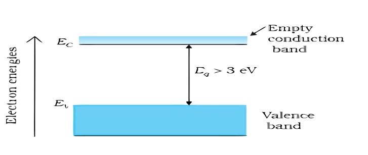
(ii)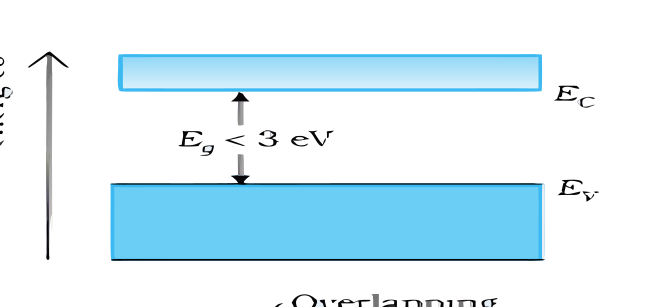
(iii)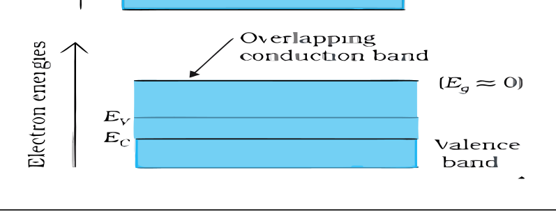
All Semiconductor Electronics: Materials, Devices and Simple Circuits questions2024 question paperNCERT solutions: Semiconductor Electronics: Materials, Devices and Simple CircuitsPractice Semiconductor Electronics: Materials, Devices and Simple Circuits →
More from Semiconductor Electronics: Materials, Devices and Simple Circuits
- With the help of a circuit diagram, explain the working of a p-n junction diode as a full-wave rectifier. Also draw its input and output waveforms.2022 · asked 2×
- State the working principle of an LED. Write any two important advantages and two disadvantages of LED.2022
- What are majority and minority charge carriers in an extrinsic semiconductor? A p-n junction is forward biased. Describe the movement of the charge…2025
- A pure Si crystal having 5 × 10^28 atoms m^-3 is dopped with 1 ppm concentration of antimony. If the concentration of holes in the doped crystal is…2024
- With the help of circuit diagrams, briefly explain the forward biasing and the reverse biasing of a p-n junction diode.2026
- In an intrinsic semiconductor, carrier's concentration is 5 × 10^8 m^-3. On doping with impurity atoms, the hole concentration becomes 8 × 10^12…2025
- Assertion: A hole is an apparent free particle with effective positive electronic charge. Reason ( R ): A hole is not necessarily a vacancy left…2025
- Explain the following, giving reasons: A doped semiconductor is electrically neutral. In a p-n junction under equilibrium, there is no net current.…2024
CBSE Class 12 Physics past-paper question from the 2024 board exam, with the answer as CBSE’s own marking scheme gives it. Where our answers come from.