✓ Board-verified
Physics · 2022 · 3 marks
Semiconductor Electronics: Materials, Devices and Simple CircuitsSemiconductor Diode3 marksUnderstandshort answer
CBSE 2022 · Region 5 · Set 1 · Q5
(i) Draw V-I characteristics of a p-n Junction diode. (ii) Differentiate between the threshold voltage and the breakdown voltage for a diode. (iii)…
(i)
Draw V-I characteristics of a p-n Junction diode.
(ii)
Differentiate between the threshold voltage and the breakdown voltage for a diode.
(iii)
Write the property of a junction diode which makes it suitable for rectification of ac voltages.
Marking-scheme solution
$\displaystyle V-I$ characteristics $\displaystyle 1$
Difference between threshold voltage and breakdown voltage $\displaystyle 1$
Property of junction diode $\displaystyle 1$
(i)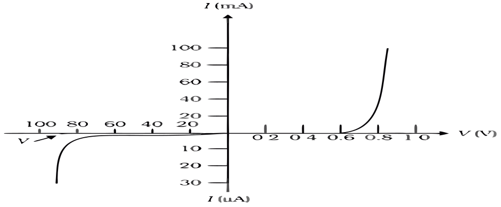
(ii)
Threshold Voltage: Forward bias voltage at which the current increases significantly (exponentially) even for a very small increase in voltage.
Alternatively:
Forward bias voltage at which the width depletion layer and barrier potential decreases significantly.
Alternatively:
The voltage at which resistance of junction decreases significantly.
Break down voltage: Reverse bias voltage at which current increases suddenly Alternatively:
Large number of covalent bonds present in the depletion layer break suddenly
(iii)
Junction Diode conducts when it is forward biased and does not conduct when reverse biased.
All Semiconductor Electronics: Materials, Devices and Simple Circuits questions2022 question paperNCERT solutions: Semiconductor Electronics: Materials, Devices and Simple CircuitsPractice Semiconductor Electronics: Materials, Devices and Simple Circuits →
More from Semiconductor Electronics: Materials, Devices and Simple Circuits
- With the help of a circuit diagram, explain the working of a p-n junction diode as a full-wave rectifier. Also draw its input and output waveforms.2022 · asked 2×
- State the working principle of an LED. Write any two important advantages and two disadvantages of LED.2022
- What are majority and minority charge carriers in an extrinsic semiconductor? A p-n junction is forward biased. Describe the movement of the charge…2025
- Draw the circuit diagrams for obtaining the V-I characteristics of a p-n junction diode. Explain briefly the salient features of the V - I…2024
- A pure Si crystal having 5 × 10^28 atoms m^-3 is dopped with 1 ppm concentration of antimony. If the concentration of holes in the doped crystal is…2024
- With the help of circuit diagrams, briefly explain the forward biasing and the reverse biasing of a p-n junction diode.2026
- In an intrinsic semiconductor, carrier's concentration is 5 × 10^8 m^-3. On doping with impurity atoms, the hole concentration becomes 8 × 10^12…2025
- Assertion: A hole is an apparent free particle with effective positive electronic charge. Reason ( R ): A hole is not necessarily a vacancy left…2025
CBSE Class 12 Physics past-paper question from the 2022 board exam, with the answer as CBSE’s own marking scheme gives it. Where our answers come from.